- Hits: 1445
RF 28.8. MHz Transceiver and RF 144 MHz Transceiver Unit Prototype
28.8 MHz Transceiver
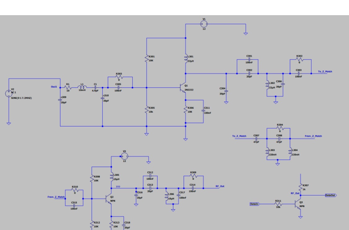
we are working on a 28.8 MHz transceiver, and instead of directly using a 7.2 MHz crystal oscillator, I designed a circuit where R1, L1, and C1 work together to generate the 7.2 MHz signal. This signal is then processed through multiple stages to achieve the desired output frequency of 28.8 MHz.

1. Oscillator Stage (R1, L1, C1 - Replacing Crystal Oscillator):
• In a traditional oscillator, a 7.2 MHz crystal would set a precise frequency, but I designed a tuned circuit instead.
• R1, L1, and C1 create an LC tank circuit, which resonates at 7.2 MHz
and sustains oscillations.
• L1 (10mH) and C1 (4.GpF) determine the oscillation frequency based on the formula: f = 1/2π rad(lc)
• C0G and C10 (20pF capacitors) help stabilize the frequency by reducing noise and unwanted harmonics.
2. Frequency Multiplier Stage (C0S, C10, R303):
• The output from the oscillator stage needs to be multiplied by 4 to reach
28.8 MHz.
• C09 and C10 help filter and amplify the fundamental 7.2 MHz signal while allowing higher harmonics to pass through.
• R303 is 0Ω, meaning it acts as a direct wire rather than a resistor. This
ensures the signal is transferred without any voltage drop.
• Q1 (2N2222 Transistor) acts as an amplifier, boosting the signal strength so that it can drive the next stage effectively.
3. Amplification and Filtering Stage (L301, L302, C301):
• The transistor Q1 amplifies the signal, but it also introduces unwanted harmonics.
• L301 (22μH) and L302 (22μH) help in filtering out undesired frequencies
and ensuring that the 28.8 MHz harmonic is dominant.
• C301 (100nF) and C302 (20pF) act as bypass capacitors, removing high- frequency noise from the power supply.
• R302 (0Ω) acts as another direct connection, ensuring maximum signal
transfer.
4. Impedance Matching Network (C307, C308, L303, L304):
• Before sending the signal to the next stage, it needs to be properly
matched to the circuit’s impedance.
• C307 and C308 (47pF each), along with L303 and L304 (220nH each), form a Pi-network to adjust the impedance and improve power transfer.
• This ensures that the signal is not distorted when it reaches the next stage.
5. Modulation and Output Stage (Ǫ2, Ǫ3, C315):
• Q2 (NPN Transistor) is used to process the modulated signal, amplifying it before transmission.
• C315 (100nF) helps block DC components, allowing only AC signals to pass.
• R311 (10kΩ) and Q3 (NPN Transistor) act as a final signal processor before sending the output signal.
• The final RF signal is sent through RF_Out, which is the transmission point of the transceiver.
we have not conducted the simulation for this circuit at this time. However, once we complete the simulation, we will analyze the results and share them accordingly.
Bushra elwane Noura Kabbara
--------------------------------------
144 MHz Transceiver
Introduction
This article describes the design and implementation of a 144 MHz Transceiver.
Requirements
In order for the system to perfectly fit the application, several requirements must be met. These requirements are stated below:
| Requirement # | Description | Date Modified |
| T144_SYS_01 | The system shall be implemented on a 1 or 2-layer PCB | |
| T144_SYS_02 | The system shall use FSK ASK mod/demod for data transmission/reception. | 28/8/2024 |
| T144_SYS_03 | ||
| T144_SYS_04 | ||
| T144_SYS_05 | The system shall have its own STM32f103C8T6 controller | |
| T144_SYS_06 | ||
| T144_SYS_07 |
HW System Design

Software Tools
Smith chart: Used to design and analyze RF circuits (specifically impedance matching networks).
LTspice: It is an electronic simulation tool used to simulate electronic circuits.

Subsystems Design
144MHz Modulation/Demodulation Scheme
